
Advanced Packaging

ASE and Amkor’s 2026 CapEx Priorities – Advanced Packaging Focus

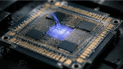
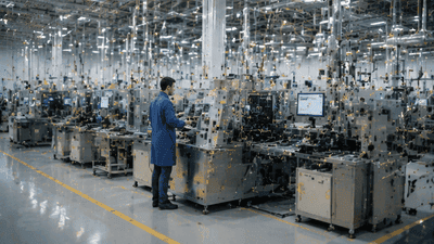
If 2025 was the year the market finally accepted that advanced packaging was no longer a niche, 2026 is the year ASE and Amkor are acting like it. Both companies are putting capital behind the same big idea: advanced packaging and heterogeneous integration are now central growth engines, not side businesses. The scale of their spending plans says as much as any earnings call or roadmap slide. In a market reshaped by AI, HPC, chiplets, and HBM, CapEx has become a statement of strategy.

Power/Signal Integrity Simulation Challenges in MCMs

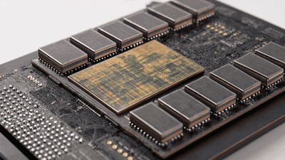
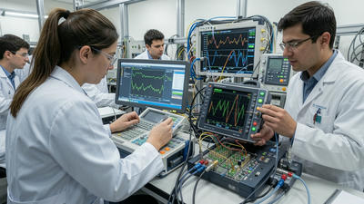
Multi-chip modules, or MCMs, have become one of the most practical forms of advanced packaging and heterogeneous integration. Instead of forcing every function onto one die, designers can place several dies side by side in the same package and connect them through an interposer, substrate, fan-out structure, or other high-density routing fabric. That flexibility is powerful, but it also creates a new class of simulation problems. Power integrity and signal integrity, once mostly chip- or board-level concerns, now have to be solved inside a tightly packed multi-die environment.

Upgraded EMC Material Requirements in Advanced Packaging

Advanced packaging has changed the way semiconductor systems are built, and with that change has come a quieter but equally important evolution in materials. One of the most overlooked heroes in the entire stack is EMC, or epoxy molding compound. In simple packages, EMC was mostly a protective shell. In advanced packaging and heterogeneous integration, it has become a structural, thermal, mechanical, and reliability-critical material that helps make the whole system viable.

CoWoS Packaging Capacity Doubles in 2026, Yet Supply Gap Remains

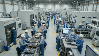
In 2026, the semiconductor industry hit a milestone that would have seemed ambitious only a few years ago: the global capacity for chip-on-wafer-on-substrate, or CoWoS, advanced packaging roughly doubled. By any traditional metric, that should have eased the pressure on cutting-edge compute supply. Yet, in practice, the opposite is happening. Despite this dramatic expansion, demand for CoWoS capacity still outstrips supply, and the gap is reshaping strategies across the semiconductor ecosystem.

Competitive Landscape of Advanced Packaging: The Coopetition Between OSATs and Foundries

Advanced packaging has moved from the back end of semiconductor manufacturing to the center of the industry’s strategic map. As AI, high-performance computing, mobile systems, automotive electronics, and chiplets all push toward heterogeneous integration, one question has become unavoidable: who owns the packaging layer of the future, OSATs or foundries? The answer is not a clean winner-takes-all outcome. It is a complex and evolving contest of overlap, specialization, and cooperation. In other words, it is cooptition.

New Standards for Cleanroom Grades and Environmental Requirements in Advanced Packaging

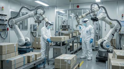
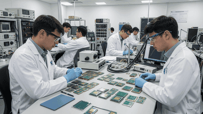
Advanced packaging has changed the rules of semiconductor manufacturing, and cleanroom standards are changing with it. What used to be a largely front-end concern is now a packaging concern too, because heterogeneous integration depends on much more than just transistor quality. It depends on the cleanliness of bonding surfaces, the stability of thin wafers, the behavior of mold compounds, the integrity of fine-pitch interconnects, and the control of particles, humidity, and temperature throughout assembly. In short, the environment has become part of the design.

Surging Demand for Laser Drilling and Plasma Dicing Equipment in Advanced Packaging

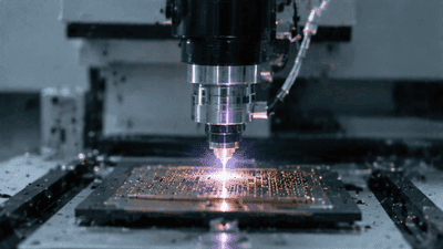
Advanced packaging has become one of the semiconductor industry’s most important growth engines, and it is now pulling a surprising set of process tools into the spotlight. Among the most in-demand are laser drilling and plasma dicing equipment. These machines sit close to the heart of heterogeneous integration, fan-out packaging, wafer thinning, TSV formation, glass substrate processing, and other advanced flows where precision, yield, and throughput matter enormously. As packaging moves from a back-end afterthought to a strategic platform, the equipment used to shape, open, and separate materials has become just as important as the dies themselves.

Chiplet Ecosystem Standardization: UCIe Alliance’s 2026 Milestones

By 2026, it has become clear that the future of advanced encapsulation and heterogeneous integration will be defined as much by standards as by process technology. Universal Chiplet Interconnect Express, or UCIe, sits at the center of this transformation. Launched as an open die-to-die interconnect specification for chiplets, the UCIe Alliance has now accumulated several generations of specifications and ecosystem deliverables that are reshaping how the industry thinks about system design, advanced packaging, and multi-vendor chiplet interoperability.

  • 1
  • 2
  • 3